 www.jyu.fi
First Experimental Realization of Two-Dimensional Topological Crystalline Insulator
Ask AI about this cluster
Analyzing cluster data...
Referenced clusters:
Something went wrong. Please try again.
Cluster AI
Ask questions about this threat cluster with AI-powered analysis.
Get Researcher $29.99/moArticle Content
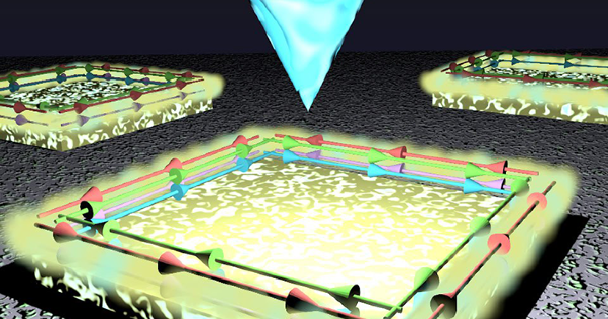
Researchers from the University of Jyväskylä and Aalto University have successfully created a two-dimensional topological crystalline insulator, a quantum material predicted over a decade ago. The material, consisting of a bilayer of tin telluride (SnTe) on a niobium diselenide (NbSe₂) substrate, was fabricated using molecular beam epitaxy. The team observed pairs of conducting edge states within a large electronic band gap exceeding 0.2 eV, which are protected by the crystal lattice's symmetry. The SnTe film experiences compressive strain from the substrate, crucial for stabilizing its topological phase. This breakthrough allows for the tuning of the edge states through strain, which could have significant implications for future quantum electronics. The findings were published in Nature Communications.
Key Points: • First experimental realization of a two-dimensional topological crystalline insulator. • Conducting edge states observed within a band gap exceeding 0.2 eV. • Strain from the substrate is essential for stabilizing the topological phase.